Tutorial #3
Drawing Physical Layout and Performing DRC
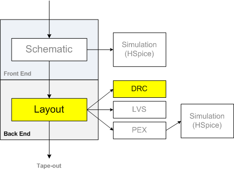
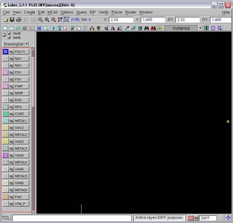
如果 Tutorial 01 & 02 已經確定你的INV及NAND2符合要求(input & output function是對的),即可開始畫屬於自己的 layout,這部份主要是做到 DRC,它只 check 你的 design rules 有沒有對, 並不管你 cell 的function 是否符合要求。
Please invoke Laker by typing the following command:
$ laker &
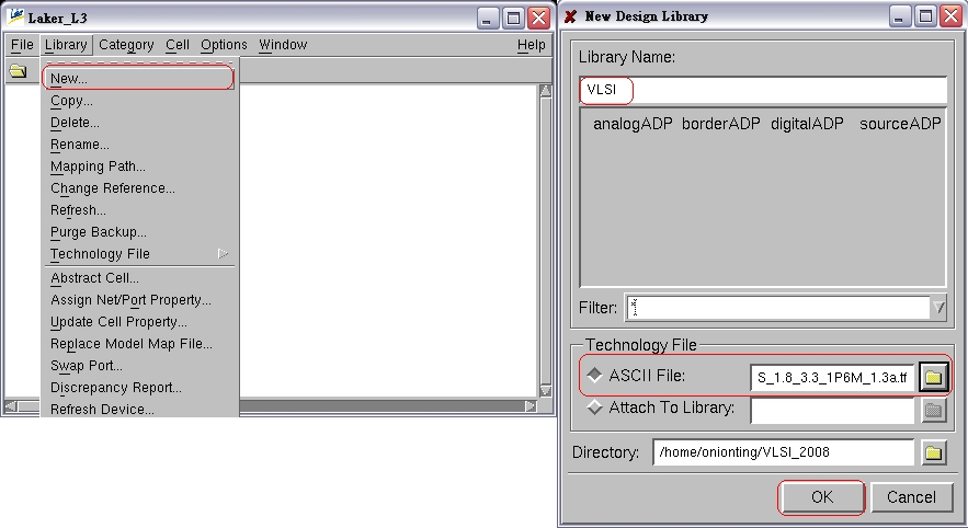
ASCII File: /home/iltseng/pub/Library/TSMC_18_technology/MM_18S_1.8_3.3_1P6M_1.3a.tf
Choose the technology file as shown below:
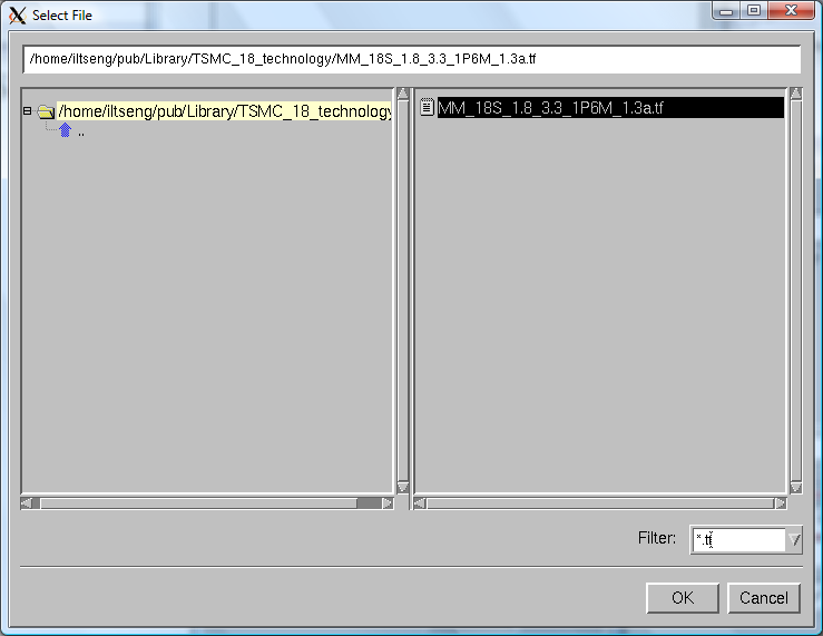
ASCII File: /home/iltseng/pub/Library/TSMC_18_technology/MM_18S_1.8_3.3_1P6M_1.3a.tf
上圖可看到很多 metal 材質列表
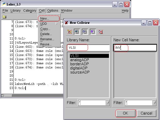
Example : INV
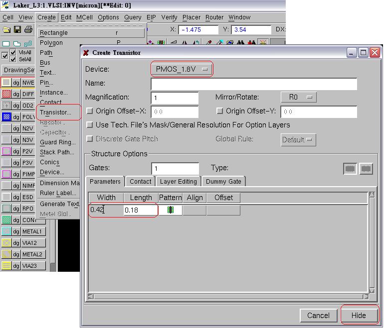
Create a PMOS transistor:
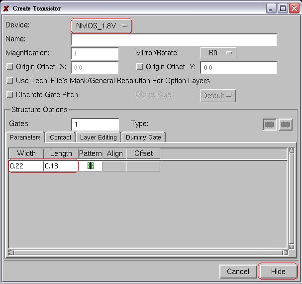
Create an NMOS transistor:
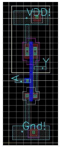
PMOS & NMOS 已完成
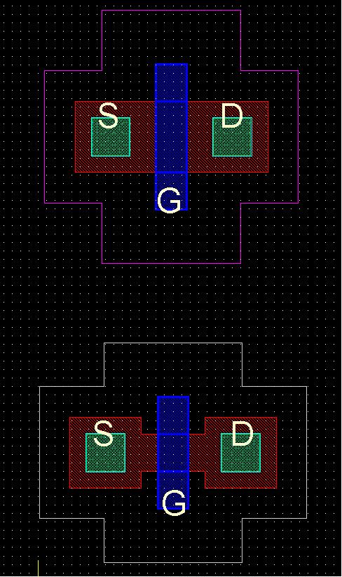
已經有PMOS和NMOS這兩個基本元件
(1) 從schematic來看,PMOS和NMOS的Gate端是相接的(材質:Poly)
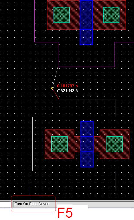
點選材質的地方(Poly),按R(可畫圖),再按F5
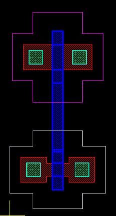
(2) 從schematic來看,PMOS : S端接VDD, NMOS : S端接Gnd, 且D端相接
(請記得畫 Nwell)
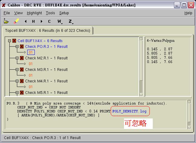
注意 : 每畫完一個步驟, 可做一次 DRC, 以確保在每個環節都符合 design rules, 不至於造成之後debug 上的困難
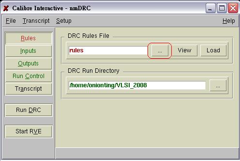
Invoke Mentor Graphics Calibre to perform design-rule checking (DRC):
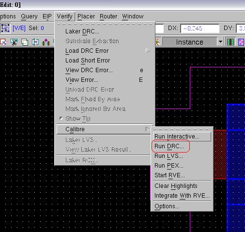
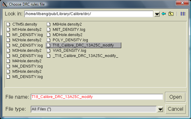
Choose DRC rules file:
Choose the following DRC rules file:
/home/iltseng/pub/Library/Calibre/drc/T18_Calibre_DRC_13A25C_modify
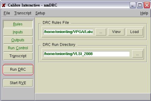
Press the "Run DRC" button to perform design-rule checking:
last update: October 14, 2009