
(1) Type the following commands on your x-terminal console:
$ icfb &
Then the following Command Interpreter Window (CIW) and the "What's New" window will show up:

Figure 1. Command Interpreter Window (CIW)
(2) You may close the "What's New" window since it will not be used in this tutorial.

Figure 2. You may close the "What's New" window
(3) Click on "File --> New --> Library ..." from the menu of the CIW window:

Figure 3. Creating a new library
Note that a library can contain a collection of your design. For example, a library can contain the cells of an inverter, a NAND gate, a NOR gate, an OR gate, an AND gate, a half adder, and a full-adder. Each of those cells may consist of its corresponding schematic, symbol of the schematic, and layout.
(4) In the "New Library" window, type "mydesign" as the Library Name. Then click on "Don't need a techfile". After that, click "OK".

Figure 4.
(5) On the menu of the CIW window, click on "Tools --> Library Manager ...".

Figure 5.
After the window of "Library Manager" shows up, you can see that the library "mydesign" has been created (as seen in the above figure).
(6) Click on "File --> New --> Cell View ..." to create a new cell (block). Then type the Cell Name as "inv". We shall use Cadence Virtuoso - Composer (a type of schematic editor) to draw the schematic of an inverter. Click "OK".

Figure 6. Creating a new cell
(7) The Virtuoso - Composer (Schematic Editor) will show up:

Figure 7. Cadence Virtuoso Schematic Editor (also known as Composer)
(8) This tutorial will show you how to draw the schematic of an inverter. First, click on "Add --> Instance..." and the following window will show up. Click on the "Browse" button to choose the Library "analogLib", the Cell "nmos4", and the View "symbol", as shown in Figure 9. Then click on "Close" button of the Library Browser. You may click on the "Hide" button of the "Add Instance" window.

Figure 8.

Figure 9.
(9) You can now place an NMOS device on the schematic.

Figure 10.
Please add instances nmos4, pmos4, vdd, and gnd only. After placing devices on the editor, connect them properly in order to form an inverter.
(10) Use "Add --> Wire" (or use the shortcut 'w'), together with mouse clicks, to connect terminals of devices (Note: Do not forget to connect body/bulk terminals to vdd or gnd.)
(11) Use "Add --> Pin" to add the input pin (Pin Name: vi) and the output pin (Pin Name: vo) of the inverter.
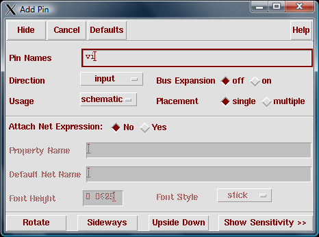

Figure 11. Figure 12.
(12) Select the NMOS/PMOS device by a mouse click and then click on "Edit --> Properties --> Objects" (or use the shortcut 'q') to specify the transistor Width and Length. Use the following values:
NMOS width: 0.22 um (type "0.22 u")
NMOS length: 0.18 um (type "0.18 u")
PMOS width: 0.42 um (type "0.42 u" as shown in Figure 13,
it will then become 420.00n M)
PMOS length: 0.18 um (type "0.18 u" as shown in Figure 13,
it will then become 0.18 u M)
The NMOS length and the PMOS length are the same (0.18 um) since the library is used for TSMC's 0.18 micron (micro meters) fabrication process.

Figure 13.
Note that you can choose Display-"both" (Figure 13) in order to show both parameter name and value in red text on the schematic editor.
(13) The completed schematic for the inverter should look like this:

Figure 14.
(14) Click on "Check and Save" to check errors of your design and the then save the design to the disk. Take a look at the CIW window to see if there are errors (Figure 15).

Figure 15. No errors were found after clicking "Check and Save"
(15) Since the schematic of the inverter has been completed and saved, the "Library Manager" window will look like this:

Figure 16.
(16) As shown in Figure 17, on the menu of Virtuoso Schematic Editor, click on "Design --> Create Cellview --> From Cellview...". The "Cellview From Cellview" (Figure 18) window will show up. Click "OK".

Figure 17.

Figure 18.
(17) On the window of "Symbol Generation Options", as shown in Figure 19, please check whether Left Pins and Right Pins are correct. In our inverter example, "vi" is the input and "vo" is the output. When we are drawing logic symbols, input terminals are usually on the left while output terminals are usually on the right. Click "OK".

Figure 19.
(18) Virtuoso Symbol Editor will then create a template for the symbol of the inverter. Note that the "vi" terminal is on the left while the "vo" terminal is on the right. We can now start editing the symbol.

Figure 20.
Tips:
To change the grid size that your mouse can move around, click "Options --> Display..." on the menu of Virtuoso Symbol Editor and change the value of "Snap Spacing" to 0.0125 or other values.
To automatically generate the red selection box that covers the entire symbol, click "Add --> Selection Box..." from the menu of Virtuoso Symbol Editor (or click on the "Selection Box" button, which is located on the left vertical toolbar), and then click "Automatic".
To add shapes, click on "Add --> Shape" and then choose the shape that you would like to add.
(19) Edit the symbol of the inverter and make it look like the one shown in Figure 21. Later on, we can build a larger logic circuit by using the inverter and other logic symbols. Click the "Save" button, which is located on the left vertical toolbar, to save your design.

Figure 21.
(20) If you go to the window of Library Manager, you can see that the "inv" cell has schematic view and symbol view. You can double-click on the schematic view or symbol view and Virtuoso will open the corresponding window (Schematic Editor or Symbol Editor) for you to view/edit the details.

Figure 22.
(22) Homework: Please draw the transistor-level schematics of a NAND gate (cell name: nand2), a NOR gate (cell name: nor2), an AND gate (cell name: and2), an OR gate (cell name: or2), an XOR gate (cell name: xor), a half-adder (cell name: half_adder), and a full-adder (cell name: full_adder). Please store all of those gates in the "mydesign" library; each gate is a Cell and each cell has a schematic and a symbol.
Tips:
The schematic of an and2 gate can be built from a nand2 gate and an inverter.
Use "Add --> Instance ..." on the menu of Virtuoso Schematic Editor to add a symbol, that has been built previously, on the schematic.

Figure 23. The transistor-level schematic of a NAND gate (cell name: nand2)

Figure 24. The logic symbol of a NAND gate (cell name: nand2)
last update: February 19, 2009